JX Advanced Metal Corps (5016.T)
The Background: Why the computing bottleneck arises?
GPT-2, released in 2019, had 1.5 billion parameters. GPT-3, released one year later, had 175 billion — a 100x increase in one step. GPT-4, released in 2023, is estimated to have somewhere in the range of a trillion parameters. In the span of roughly four years, the scale of the models driving the AI revolution grew by something close to a thousand times.
Each of those parameters is a number that need to be stored in memory, reading during every forward pass, updated during every backward pass, and synchronized across every GPU participating in training. A trillion parameters at 16-bit precision takes 2 terabytes of memory just to hold the model weight — before you account for the gradients, the optimizer states, and the activation flowing through the network during training, which together can multiply that memory requirement by six to eight times. No single machine in existence can hold this. No single GPU comes close.
So you distribute. You take thousands of GPUs, split the model and the data across them, and run training as a massive parallel operation. OpenAI reportedly trained GPT-4 on somewhere around 25,0000 A100 GPUs running continuously for months. The compute cost was in the tens of millions of dollars. This is now the baseline for frontier model training, and the model coming after GPT-4 are larger still.
Training something like GPT-4 isn't something you can do on a single GPU. The model has hundreds of billions of parameters, and the amount of memory required to hold all of them far exceeds what any single GPU can store. So engineers split the work across thousands of GPUs simultaneously.
But the moment you involve multiple GPUs, they need to constantly talk to each other. They need to share partial results, synchronize their work, and pass data back and froth throughout the entire training process. And this is where the pain starts — because not all communication channels are created equal.
Inside a single server, GPUs can talk to each other over NVLink, which is extremely fast. But the moment you need to go outside that server and talk to a GPU sitting in a different server box, you're now going through a network — InfiniBand or Ethernet — which is dramatically slower. We're talking roughly a 10x speed difference between in-server and cross server communication.
This speed gap is the structural bottleneck that plagued larger model training for years.
How to train an AI model?
When you distribute training across many GPUs, there are three main strategies for splitting the work. Each one ran into the bottleneck in a different way.
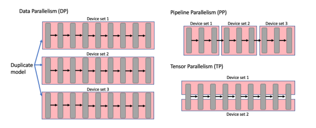
Data Parallelism is the simplest approach. You copy the entire model onto every GPU, then split your training data into chunks and give each GPU a different chunk to process. Each GPU independently computes how the model's weights should be updated based on its data chunk. Then — and this is the problem — all the GPUs have to compare notes. They need to collect everyone's computed updates, average them together, and sync up before the next rounds. This process is called AllReduce, and it requires every GPUs to send data to and receive data from every other GPU. With thousands of GPUs, the volume of cross-server communication becomes enormous. Every training steps ends with a massive collective communication event that saturates the network.
Pipeline Parallelism takes a different approach. Instead of copying the whole model everywhere, you slice it by layers and assign each slice to a different GPU. GPU 1 handles layers 1-10, GPU 2 handles layers 11-20, and so on, like a factory assembly line. Each GPU processes its section and passes the output to the next one.
The problem here is what's called the pipeline bubble. While GPU 1 is processing the first batch, GPUs 2 through N are all sitting idle waiting for input. Then when GPU 1 finishes and passes to GPU 2, GPU 1 has to wait for new data. There's always a stall somewhere in the pipeline, and the longer the pipeline — meaning the more GPUs you chain together — the worse the idle time gets. You end up with expensive hardware doing nothing for significant portions of each training step.
Model Parallelism (also called Tensor Parallelism) is theoretically the most efficient approach. Instead of slicing the model by layers, you split individual layers themselves across multiple GPUs. A single enormous matrix computation gets broken into pieces, each GPU handles pieces simultaneously, and then they stitch the results back together, Since all the GPUs are genuinely working at the same time, there's no pipeline bubble problem.
The catch is that splitting a single layer across GPUs means those GPUs need to communicate very frequently — after every computation — and the data they exchange is substantial. If the GPUs are far apart with a slow network between them, the time spent waiting for communication exceed the time spent actually computing. In practice, model parallelism was only viable within a single server where NVLink made the communication fast enough. Extending it across multiple servers through the slower network was too painful to be practical.
So no matter which strategy you used, you kept hitting the same wall: the speed different between inside-server and cross-server communication.
Why communication is so expensive?
First, the frequency. A modern transformer model might have 96 layers. With tensor parallelism, you have a synchronization event between every pair of adjacent layers. That's 96 communication rounds per forward pass, and then another 96 during the backward pass when computing gradients. Compare that to pipeline parallelism, where you might have 3 communication events total if you have 4 GPUs. Tensor parallelism is doing orders of magnitude more individual communication operations per training step.
Second, the size of the data. When GPUs synchronize their partial results after each layer, the data they're exchanging is proportional to the size of the activation — the intermediate outputs flowing through the network. In a large model, these activation tensors are enormous. Every synchronization event moves a lot of data.
Now put these two facts together and think about what happens when the GPUs are in different servers connected by InfiniBand rather than NVLink.
NVLink might give you 900 GB/s of bandwidth between GPUs. InfiniBand might give you 400 Gb/s, which is aroung 50 GB/s. That's roughly an 18x difference in bandwidth. And latency — the delay before data even starts moving — is also higher over Infiniband.
With tensor parallelism doing a synchronization every single layer, and each synchronization moving a large chunk of data, the time spent on communication between servers adds up extremely fast. On each training step, the GPUs might spend more time waiting for cross-server synchronizations to complete than they spend doing actual matrix multiplications. At that point you've bought expensive hardware and it's mostly sitting idle waiting for the network. The math doesn't work.
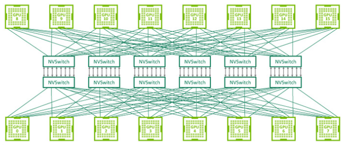
Linking the GPUs: What actually NVLink (NVL72) does?
The GB200 NVL72 does not optimize communication across the speed gap. It eliminates the gap.
The system puts 72 Blackwell GPUs and Grace CPUs inside a single rack, and then connects all 72 GPUs together with NVLink through 9 NVSwitch trays. Every single GPU in the rack is on the same NVLink fabric. There is no server boundary to cross. There is no slow network hop between any pair of GPUs, because all of them are reachable via NVLink.
The 9 NVSwitch trays create 1,296 NVLink ports total, which matches a structure where each of the 72 GPUs has NVLink connections. This is designed specifically so that communication between any two GPUs in the rack never has to compete with or block communication between any other two GPUs. The full bandsidth is available to everyone simultaneously, no matter how many GPU pairs are talking at the same time.
The "Shared memory space" framing in the text is describing something more conceptual than literal. The GPUs each have their own physical memory, but because NVLink is so fast, a GPU reading data from another GPU's memory on the other side of the rack experiences latency and bandwidth that approaches what you'd get reading from your own local memory. From a programming standpoint, software can treat all 72 GPUs as if they're sharing a single enormous memory pool, which is a fundamentally different and much simpler way to think about distributing a model.
How NVL72 was applied to training method?
The reason model parallelism was painful before was that splitting a single layer across multiple GPUs forced frequent high-bandwidth communication, and that communication was slow whenever it had to cross server boundary. With NVL72, there are no server boundaries within the rack. You can split a model's layers arbitrarily across all 72 GPUs and the inter-GPU communication strays on NVLink the whole time. The communication is fast enough that it no longer dominates the training step.
This is what the "model parallel configuration at single-GPU efficiency" means. When a model runs on one GPU, all memory access is local — there's zero communication overhead. NVL72 brings 72 GPUs as close to that ideal as physically possible. The GPUs spend far more of their time actually computing and far less time waiting on each other.
In practical terms. this means you can train models with hundreds of billions of parameters inside a single rack without the training process constantly stalling at communication barriers. The GPUs stay busy. Utilization goes up. you either train faster with the same number of GPUs, or you train larger models that simply wouldn't have been tractable before.
The conceptual shift is that Nvidia moved the boundary of "one computer" from the server to the rack. Everything inside the rack behaves like a single machine. The network problem doesn't go away entirely — you still need to connect multiple racks together for the largest clusters — but the bottleneck has been pushed further out, and within that rack the hardware can be used closer to its theoretical maximum.
So, Problem Solved with NVL72?
NVL72 puts 72 GPUs in one rack and connects them all with NVLink, so tensor parallelism can scale across all 72 GPUs without touching a slow network. That sounds like a clean solution. But there's a physical problem hiding underneath it that haven't talked about yet.
When those 72 GPUs communicate over NVLink inside the rack, they're sending enormous amounts of data at extremely high speeds. NVLink give around 900 GB/s per GPU. With 72 GPUs all talking to each other simultaneously through those NVSwitch trays, the total data moving around inside that rack at any given moment is staggering — we're talking multiple terabits per second of aggregate traffic flowing through the interconnect fabric.
That data has to travel somewhere physically. And the way data has traditionally traveled inside servers and racks is through copper wires.
The Bottleneck: How data centers work and Why copper doesn't suffice
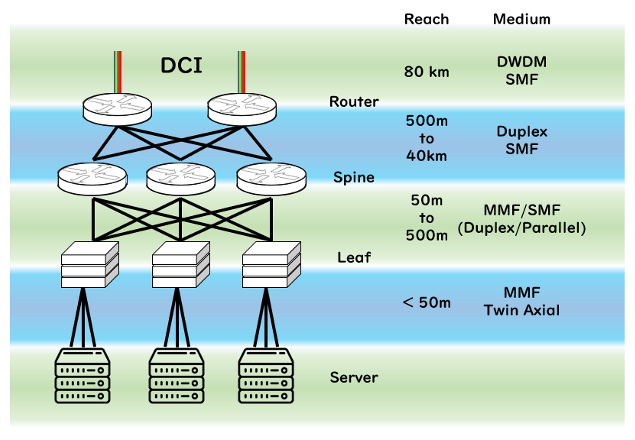
- Layer 0: Insider the server: GPU to GPU with in a single node
This is the innermost level, before you even reach a network switch. Inside one server, GPUs talk to each other directly over NVLink through NVSwitch chips on the motherboard.
The distances here are centimeters. A GPU die to a neighboring NVSwitch chip on the same board might be 5 to 15 centimeters apart. At these distances, copper traces on the circuit board work fine. This is why NVLink has always worked well within a single server. The architecture was designed for this scale. The bandwidth is enormous — 900 GB/s per GPU — because copper can deliver that at centimeter-scale distances without fighting against its own limitations.
Communication at this layer is entirely electrical. No optics involved.
- Layer 1: The ToR Switch: Server to Top-of-Rack
At thje top of each rack sits what's called a ToR switch — Top of Rack. Every server in that rack connects up to this switch. This is the first point where traffic from individual servers aggregates before going everywhere else.
The distances here are vertical — from a server unit near the bottom of a 42U rack up to the ToR switch at the top. That's somewhere between half a meter and two meters of cable. At this scale, you're typically still using copper, but in a more sophisticated form. Direct Attach Copper cables — DAC cables — handles most server-to-ToR connections. These are passive copper cables with transceivers built directly into the ends, and they work well at speed up to 400 Gb/s for distances under about 5 meters.
For the fastest connections — particularly when you're connection GPU servers running NVLink at full speed up to the ToR — even DAC starts to struggle. The signal speeds required mean you need Active Copper Cables, which have small amplifier chips embedded in the cable itself to compensate for signal degradation. Those amplifiers consume power, but the distance are short enough that it's still manageable.
Some deployments at this layers are already moving to optical transceivers, particularly for the highest-speed links. But the dominant approach is still copper because the distances are short enough to make it work.
The bandwidth at this layer is already substantial. A single high-end ToR switch might have 64 ports running at 400Gb/s each, giving a total switching capacity of over 25 Tb/s. Every GPU server in the rack in connected here, and all their traffic enters the network through these links.
- Layer 2: The Leaf Switch: ToR to Leaf
In AI data center deployments, the architecture often adds a Leaf layer between to ToR switches and the Spine. All the ToR switches in a cluster of racks connect up to Leaf switches. A Leaf switch might aggregate traffic from 8 to 16 racks worth of ToR switches.
This is where distances start to become genuinely challenging for copper. The cables running from a ToR switch at the top of one rack to a Leaf switch in a central switching row migh run 10 to 30 meters. At that distance and at speeds of 400 Gb/s or 800 Gb/s per link, copper is no longer viable.
This is the transition point. From the Leaf. From the Leaf layer upward, the connections are optical. You use optical transceivers — small pluggable modules that convert electrical signals from the switch chip into light, send that light through fiber, and convert it back to electrical at the other end.
The fiber cables themselves are cheap and the light travels through them with essentially no degradation. But those pluggable transceiver modules — the components doing the electrical-to-optical conversion — are where the power cost lives. Each transceiver module consumes several watts just to do the conversion. A Leaf switch with 64 uplink ports might have 64 transceiver modules, consuming hundreds of watts collectively just for signal conversion, before you even count the switching chip itself.
The traffic pattern at this layer is also shifting from what lower layers see. Within a rack, most traffic is between GPUs in the same training job — dense, high-bandwidth, all-to-all communication patterns driven by tenseor parallelism happening over NVLink. By the time traffic reaches the Leaf layer, it's the communication that couldn't stay within a rack — gradient synchronization across rack boundaries, parameter server traffic, and so on. This traffic is still enormous in aggregate but has slightly different timing pattern.
- Layer 3: The Spine Switch: Leaf to Spine
Spine switches sits at the top of the hierarchy. Every Leaf switch connects to every Spine switch. In a large AI cluster, you might have 8 to 16 Spine switches, and every one of them is connected to every Leaf switch in the data center.
The distances here can be substantial. 30 to 100 meters of fiber runs through cable trays across the ceiling of a large data center floor. At these distances and speeds, optical fiber is the only option. This has been true for a long time. Nobody debates whether to use cooper at the Spine layer. It's optical by default.
The bandwidth at Spine is aggregated from everything below. A Spine switch in a large AI cluster might have hundreds of ports running at 400 Gb/s to 800 Gb/s each. The total throughput of a single Spine switch can reach petabits per second when you add up all the ports.
The challenge at Spine isn't the medium. The fiber works fine. It's the sheer scale of the switching hardware and the power consumed by the transceiver at every port. A Spine switch with 512 ports, each needing its own optical transceiver module, has 512 transceiver modules consuming power just to convert signals. At several watts per modules, that's several kilowatts of power for conversion alone on a single switch.
The Bandwidth Cliff
At Layer 0, insider the server, NVLink gives 900 GB/s per GPU. With 72 GPUs in an NVL72 rack, the aggregate internal bandwidth is in the tens of terabits per second. At the ToR switch connecting that rack to the network, the total uplink bandwidth is whatever the ToR switch can provide — maybe 12.7 Tb/s or 25.6 Tb/s on a high-end switch.
At Leaf, you aggregate multiple ToR switches, but you're still limited b y the uplink bandwidth from Leaf to Spine.
At Spine, everything aggregates, but you're limited by how many ports and how much switching capacity the Spine switches have.
At every transition between layers, there's a reduction. You never have as much bandwidth going up as you have at the layer below. This is intentional and unavoidable — you can't afford to have the same aggregate bandwidth at the top as you have at the bottom. But what matters for AI training is how large that reduction is, and how much latency each hop introduces.
When tensor parallelism is happening across racks — when a training job's GPUs are split across multiple racks and need to synchronize after every later — the traffic has to go all the way from GPU to ToR to Leaf, Leaf to Spine, Spine to Leaf, Leaf to ToR, ToR to GPU. Every one of those hops introduces latency. Every bandwidth limitation at any hop creates a potential bottleneck.
This is exactly what makes cross-rack tensor parallelism so painful. The bandwidth available at any network hop is a small fraction of what NVLink provides inside the rack, and the roundtrip through the full Leaf-Spine structure adds latency that, when multiplied by thousands of synchronization events per training step, adds up to a significant slowdown.
Where CPO enters the picture and why it matters at each layer?
CPO addresses the fundamental conversion cost — the power and latency overhead of going from electrical to optical — by moving that conversion boundary as close to the chip as physically possible.
At the ToR layer, CPO in the switch chips means that traffic from the GPU serves enters the switch, get processed, and leaves toward the Leaf layers as light without ever going through a separate pluggable transceiver module. The conversion happens inside the switch package. This eliminates the transceiver module power overhead at every port and allows the switch to handle higher aggregate bandwidth without the power budge exploding.
At the Leaf layer, the CPO in the switch chips means that the aggregated traffic from many ToR switches get forwarded toward Spine with dramatically lower power consumption per bit than traditional pluggable transceivers. As port speed move from 400 Gb/s to 800 Gb/s to 1.6 Tb/s — whitch is the direction the industry is heading — the power savings from CPO versus pluggable transceivers become proportionally larger, because the conversion cost of traditional transceivers scale with speed while CPO's does not the same degree.
At the Spine layer, CPO enables the switching capacity to scale to levels that would be impossible with traditional transceivers, If each port on a 512-port Spine switch needs a pluggable transceiver consuming 5 to 10 watts, that's 2.5 to 5 killowatts just for the transceivers on one switch. Move to 1.6 Tb/s ports and those numbers get worse. CPO brings that power cost down substantially, which is what makes feasible to build Spine switches with the port counts and speed that exabyte-scale AI training requires.
In shorts, NVLink and NVSwich solve the within-rack communication problem by eliminating the slow network for that traffic entirely. CPO solves the cross-rack communication problem by marking the Leaf-Spine network fast enough, dense enough, and power-efficient enough to handle the remaining traffic that does have to traverse the network — at the bandwidth and latency that AI training at scale actually requires.
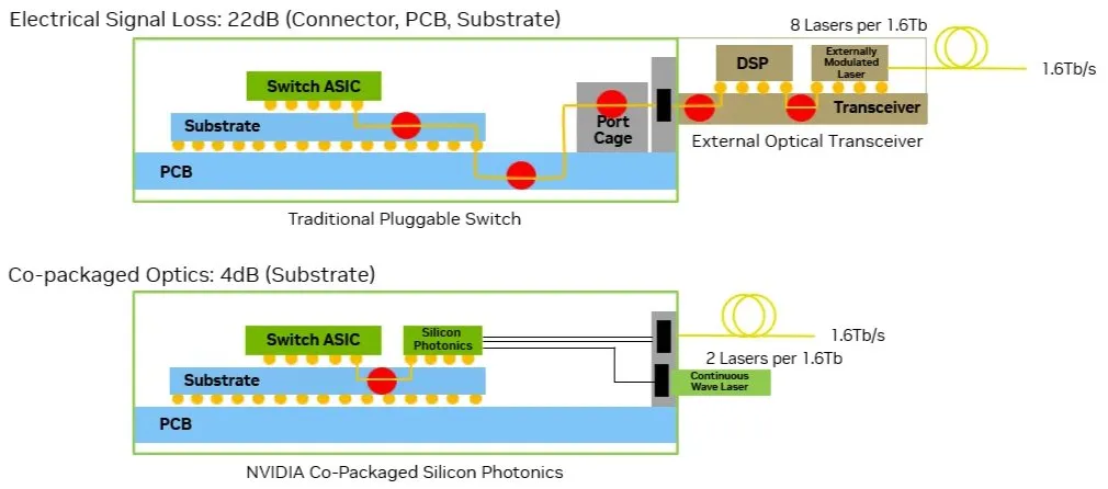
How exactly CPO change the chip?
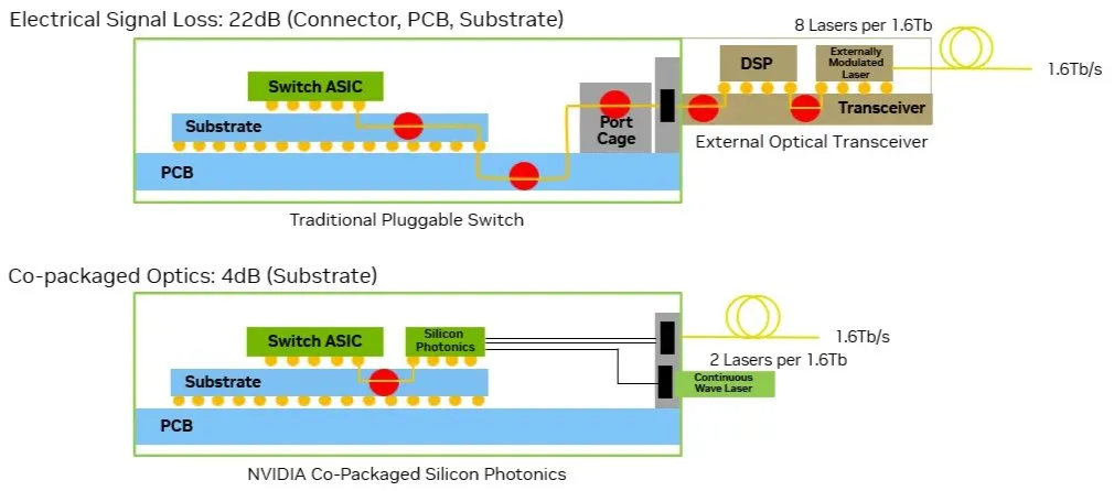
Look at the top diagram and the path the signal has to take. It starts at the Switch ASIC on the far left. The ASIC is the chip doing all the data processing. It needs to get its data out to the network, and that data starts as electrical signals.
Now trace the journey. The signal leaves the ASIC, travels down through the Substrate (the package the chip sits in), then through the PCB (the main circuit board). That's already a meaningful electrical journey through layers of metal traces. Then it has to travel across the PCB to reach Port Cage — that's the metal slot at the edge of the board where the pluggable transceiver get inserted.
At the port cage, the signal crosses a connector. Connectors are notoriously bad for high-speed signals because they introduce reflection and impedance mismatches.
Then the signal enters the External Optical Transceiver, which is that separate module on the far right. Inside the transceiver, the signal first hits a DSP — a Digital Signal Processor. The DPS's only job is to clean up the mess. By the time the signal arrived, it had been so degraded by all the copper, vias, connectors, and PCB traces that it was barely usable. The DSP reconstructs it, amplifies it, and reshapes it.
After the DSP cleans the signal, it finally reaches the Externally Modulated Laser, which converts the electrical signal into light. That light goes into the fiber and leaves at 1.6 terabits per second.
Add up the total electrical signal loss along this entire path: 22 dB. To put it in context, every 3 dB of loss means the signal has been cut in half. So 22 dB means the signal has been reduced to roughly 1/150th of its original strength by the time it reaches the laser. The DSP has to do a tremendous amount of work to recover usable data from that.
And critically, this design needs 8 lasers per 1.6 terabits. Each laser handles a fraction of the total bandwidth, and you need many of them working in parallel.
The CPO approach: and Why this structural change makes everything more efficient?
Now look at how short the journey is in the bottom diagram. The Switch ASIC is the same chip doing the same data processing job. But sitting right next to it, on the same substrate, is a chip labeled Silicon Photonics. That's the PIC which routes and modulates light. The electrical signal leaves the ASIC, travels a tiny distance through the substrate, and immediately enters the PIC. There's no long PCB trip. No port cage. No connector to cross. No external transceiver module sitting at the edge of the board. No DSP needed to clean up a mangled signal, because the signal never had a chance to get mangled in the first place.
The total electrical signal loss along this path is 4 dB. To put that in perspective: 4 dB of loss means about a quarter of the signal strength is lost. Compare that to the traditional design's 22 dB, which means roughly 99.3% of the signal strength has been destroyed by the time it reaches the laser. The CPO signal arrives at the optical conversion stage in nearly pristine condition. The traditional signal arrives essentially in ruins, and the only reason it works at all is that the DSP performs heroic computational reconstruction to recover usable data from the wreckage.
There's a second structure change visible in the diagram, and it's just as important as the path shortening. Look at the laser arrangement on the right side. A Continuous Wave Laser sitting outside the package, feeding light into the silicon photonics chip through a fiber. This is the External Laser Source design. The laser doesn't generate modulated, data-carrying light. It just produces a stead, continuous beam. The silicon photonics chip then takes that steady beam and adds the data onto it using on-chip modulators, splitting the single incoming beam into many channels and imprinting different data streams onto each one. Because one laser can feed many channels through this splitting-and-modulating arrangement, you only need 2 laser to handle 1.6 terabits, compared to 8 lasers in the traditional design where each laser had to be individually modulated for its own dedicated channel.
Now connect these two structural changes: the shortened electrical path and the externalized continuous-wave laser.
Power consumption collapses. Two things were burning enormous amounts of power in the traditional design. The first was the DSP, which had to work exponentially harder as speeds increased to reconstruct signals that had been mauled by the long electrical journey. The second was running 8 individually modulated laser per 1.6 terabits, each consuming its own power budget. CPO eliminates both. The DSP isn't needed because the 4 dB signal doesn't require reconstruction. The laser power drops by 4x because the architecture uses 2 external lasers instead of 8 internal ones. Together, these saving transform the per-port power consumption from something that would break the data center's power budge at 3.2 Tbps and beyond, into something that scales gracefully with each new bandwidth generation.
Bandwidth density increases dramatically. This is where the architectural simplification really shows. In the traditional design, every fiber connection required a port cage at the edge of the board, a connector to plug into, and an external transceiver module sticking out. Those physical components take up real estate. You can only fit so many port cages along the perimeter of the board, which caps the number of fibers you can run from a single switch. With CPO, the optical exit point is right at the package itself. Fibers come straight out of the silicon photonics chip into a fiber array. No port cages, no connectors, no pluggable modules. The same physical area can host many times more fiber connections, allowing the switch to scale to far higher aggregate bandwidth without growing in physical size.
Cost per bit drops at scale. Pluggable transceiver modules at 1.6 Tbps are extraordinarily expensive — they contain their own DSPs, their own lasers, their own packaging, their own connectors. A single high-end transceiver can cost thousands of dollars, and a high-end switch needs hundred of them. CPO consolidates the optical functionality into the silicon photonics chip and the external laser source, both of which can be manufactured at scale using established semiconductor processes. The economics flip from "buy hundreds of expensive modules per switch" to "integrate optics directly into the package," and as production volumes ramp up, the cost per bit transmitted falls steeply.
The deeper point is that all three of these efficiency gains — power, density, and cost — come from the same underlying structural change. The traditional designed accepted massive signal loss as a given built an entire compensation infrastructure around it. The DSP, the modulated laser per lane, the elaborate transceiver module, the careful PCB engineering — all of it exists to fight the consequences of routing high-speed electrical signals over board-level distances through connectors. CPO refuses to accept that signal loss in the first place. By brining the silicon photonics chip directly next to the ASIC and externalizing the laser as continuous-wave source, the design eliminates the problem rather than compensating for it. Once you've eliminated the problem, you no longer need the compensation infrastructure, and all the efficiency gains follow as a consequence.
This is why CPO isn't just an incremental improvement. It's a fundamentally different relationship with the physics of high-speed signaling. The traditional approach hits a wall as bandwidth requirements keep doubling — 600 Gbps to 1.6 Tbps to 3.2 Tbps to 6.4 Tbps — because each doubling makes the signal degradation problem worse and the compensation cost more expensive. The CPO approach scales with that doubling because it isn't fighting the same battle. The electrical path stays short, the signal stays clean, the DSP stays unnecessary, and the laser count stays low. Every generation of bandwidth scaling that would crush the traditional design simply rolls off the CPO design without breaking it.
That structural advantage is what makes CPO not merely efficient but inevitable for the AI infrastructure buildout. The traditional design works at today's speeds. It doesn't work tomorrow's. CPO works at both, and beyond.
The specific structure inside a CPO system
CPO is a careful arrangement of multiple specialized components, each made from a different material, each handling a specific part of the electrical-to-optical-to-electrical journey.
At the heart of a CPO module sits the switch ASIC or compute chip — the silicon die that handles the actual data processing. Historically, this chip sent data out through electrical signals on copper traces running across the PCB to a transceiver at the edge of the board. The signal leaves the ASIC, divides down through the substrate and PCB, travels across to the port cage at the edge, crosses a connector, and finally enters the external transceiver where it gets converted to light. In a CPO design, the ASIC is instead surrounded by photonic components packaged into the same module, drastically shortening the electrical path before signals become light.
Right next to the ASIC sits Photonic Integrated Circuit, called the PIC (Silicon Photonics on the bottom diagram). The Silicon Photonics is a silicon chip. It's built using a process where waveguides, modulators, splitters, and photodetectors are fabricated on a silicon substrate using techniques borrowed from standard chip manufacturing. Its job is to take light, manipulate it, rout it through dozens of channels, encode data onto it via modulators, and direct the resulting signals out to optical fibers. It also receive incoming light from fibers, separates the channels, and converts the light back to electrical signals using on-chip photodetectors.
The silicon Photonics is impressive at what it does. It can route, split, modulate, and detect light with extraordinary precision. But it has one critical limitation: it cannot generate the light it manipulates. This is the silicon bandgap problem. Silicon's indirect bandgap means electron transitions release energy primarily as heat rather than as photons, making silicon a fundamentally poor light emitter. Silicon photonics can do almost everything optical except produce the original light source.
That's where the External Laser Source, the ELS, comes in. In the diagram, the ELS appears as the "Continuous Wave Laser". It contains the actual laser — a small InP-based device that generates a continuous, stable beam of light at the right wavelength, typically around 1310 nanometers for data center application. The ELS sits in the same package as the ASIC and PIC, but it's deliberately kept slightly separate. There are two reasons for this physical separation. First, lasers are temperature-sensitive — their wavelength drift with heat, and the switch ASIC right next to them runs hot. Keeping the laser slightly distant gives it thermal isolation. Second, lasers have a different reliability profile than digital logic. They can fail independently and may need to be replaceable, so designers often keep them as discrete component rather than fully integrating them into the PIC.
The light flow through the system goes like this. The ELS generate a continuous wave of laser light, like a flashlight that never turns off. That light is coupled into the silicon PIC. The PIC then takes this raw light and uses its modulators to imprint data onto it, switching the light on and off or shifting its phase billions of times per second to encode the bits being transmitted. The encoded light is split into multiple parallel channels and routed to fiber connectors at the edge of the package. From there it leaves the rack entirely, traveling through fiber to wherever it needs to go in the Leaf-Spine network. In the reverse direction, incoming light from external fibers enters the PIC, get routed to on-chip photodetectors, and converts back to electrical signals that feed into the ASIC.
Where JX Advanced Metals sits in
So the architecture has three distinct material domains. The compute and switching is done in silicon ASICs — That's the TSMC. The light routing, modulation, and detection is done in silicon photonics PICs — That's a specialty silicon process run by companies like Tower Semiconductor and GlobalFoundries. The light generation is done in InP-based ELS module. That's a completely different material world with a completely different supply chain. Each material does what it does best, and the system as a whole works because all three are co-packaged.
The ELS is the only non-silicon component in the entire CPO module.
Zoom in further on how that InP laser actually get manufactured. The laser device itself — the structure that produces and amplifies light — is built by epitaxially growing thin layers of compound semiconductors on top of a starting wafer. That wafer is a single-crystal slab of Indium phosphide. Companies like Coherent and Lumentum takes these wafers and grow the laser structures on top, then process them into individual laser devices that get packaged into the ELS modules that ultimately go into CPO systems. But before any of that happens, somebody has to grow the InP crystal and slice it into wafers in the first place.
That somebody is JX Advanced Metals
The Competitive structure
The InP substrate market is genuinely concentrated. The top four producers — Sumitomo Electric, JX Advanced Metals, AXT (operating through its Beijing-based subsidiary Tongmei), and Coherent — control roughly 80% to 95% of global production capacity. Sumitomo holds the largest single share at roughly 30%, JX is the second-largest merchant supplier, AXT has historically rounded out the leading group, and Coherent is primarily a vertically-integrated producer for internal laser consumption. Chinese suppliers like Yunnan Germanium, Zhuhai DT Wafer-Tech, and Guangdong Pingrui collectively hold less than 10% and operate at production volumes an order of magnitude below the leaders.
What makes this market interesting is not the headline concentration. It's that within those four leading players, every single one has either a structural constraint or a strategic positioning issue that's reshaping who actually captures the incremental demand wave.
What's happening to JX: Three capacity expansion in one year, and counting
JX has been the most aggressive of the merchant substrate suppliers in scaling capacity, and the pace has accelerated substantially over the past year. The expansion sequence at the Isohara Plant in Ibaraki Prefecture tells the story:
On July 23, 2025, JX annouced an inital ¥1.5 billion (about $10.2m) capital investment to increase indium phosphide substrate production capacity by about 20% at is Isohara Plant. Anticipating continued high demand for InP substrates in the future, it is also considering future investments, to be made flexibly as needed.
Just over two months later, in October 2025, JX expanded that commitment. Including the ¥1.5 billion investment announced on 23 July to expand capacity by about 20%, the total capital investment is now about ¥3.3 billion to increase InP substrate production capacity by about 50% compared to 2025 levels. The capacity increase target effectively doubled within a single quarter.
Then in late December 2025, JX signaled a third expansion. JX Advanced Metal plans a third increase this fiscal year in production capacity for optical communications materials to meet rising demand from AI data centers. JX Advanced Metals has already outlined two capacity this year, with combined spending of 4.8 billion yen, lifting output by 50% by fiscal 2026. President Yoichi Hayashi said at least one more expansion will be revealed before the end of fiscal 2025, with total additional investment likely to reach several billion yen.
The pattern is significant. JX is not announcing a single large expansion and then waiting for the demand to materialize. They're announcing incremental expansions sequentially, with each new announcement upping the prior commitment as customer order visibility improves. This is exactly the behavior you'd expect from a supplier whose order book is filling faster than their announced capacity can absorb.
The financial picture supports this, JX raised its FY2025 full-year forecasts in November 2025, citing faster-than-expected demand growth in ICT materials segment for AI server applications. Total revenue now projected at ¥820 billion, operating profit ¥150 billion, and an increased dividend forecast of ¥27 per share. The timeline shows a phased payoff: minor near-term dilution from new equipment, with the bulk of the capacity ramp and its financial benefits arriving in fiscal 2027 and beyond. The capacity expansions hit the income statement in 2027 — exactly when CPO commercialization moves from early adoption into mainstream deployment, and when Nvidia's Feynman architecture and scale-up CPO rollouts start pulling additional optical I/O demand through the laser supply chain.
What's happening to AXT — China export problem is real but is showing some recovery
The AXT story is more nuanced than the simple "blocked by export controls" framing suggested earlier. The export permits have started flowing, but irregularly, and the recovery is partial.
The trajectory through 2025 was painful: Q4 2025 revenue was $23.0 million, compared with $28.0 million for the third quarter of 2025 and $25.1 million for the fourth quarter of 2024. Q4 revenue was below the initial guidance of $27-30m, due mainly to fewer than expected export control permits for indium phosphide being issued by China's Ministry of Commerce. Full year 2025 revenue came in at $88.3 million
The early 2026 picture is meaningfully better. For first quarter 2026, AXT reported revenue of $26.9 million, up 17% on $23m last quarter and 39% on $19.4m a year ago, and slightly above the forecasted $26m as export permits came in slightly better than guidance. Indium phosphide has rebounded from $3.8m (under a fifth of total revenue) a year ago, then $8m last quarter (under a third of revenue).
The forward looking guidance is more optimistic still. For Q2/2026, AXT expects growth in revenue to potentially $34m (contingent on export permits), driven primarily by record InP revenue of over $17m due to record InP order backlog exceeding $100m. Revenue from China's InP-based laser sector is expected to double again in Q2.
So AXT is recovering, but the recovery is critically dependent on three factors that don't reflect well in customer qualification decisions for production CPO grograms:
First, the export permit process remains opaque and unpredictable. AXT's Q4 2025 disappointment came after a strong Q3, illustrating that even within a single year the permit flow can swing dramatically. Customers designing CPO production schedules around 2026-2027 deliveries cannot tolerate that volatility.
Second, AXT's growth is increasingly being driven by Chinese domestic demand rather than exports. The Chinese hyperscalers — Alibaba, Tencent, Baidu, ByteDance — are building out their own AI infrastructure and want domestic suppliers. "Our revenue related to the data-center market in China is expected to grow by more than 60% in Q1 over Q4, highlighting both increased investment in these tier-1 data centers as well as the strong desire for Chinese domestic suppliers to secure local stores at every level of the AI infrastructure supply chain." This is a real business, but it's a different business than supplying Coherent, Lumentum, and the laser ecosystem feeding Nvidia and Broadcom. The structural bifurcation between Chinese-domestic and Western-customer supply chains is becoming explicit at AXT.
Third, AXT's capacity expansion is meaningful but doesn't change the export permit constraint. Since October, AXT has added about 25% more capacity, and is on track with its current plan to double capacity from Q4/2025 by the end of 2026, supporting a $35m quarterly InP revenue run-rate. The capital raise — $632.5 million — funds this expansion. But adding capacity in China doesn't solve the permit issue for non-Chinese customers. It actually amplifies the bifurcation: AXT can supply more capacity to Chinese customers reliably, but Western customers still face the same permit uncertainty regardless of how big AXT's factories get.
What's happening to Sumitomo Electric: racing to catch up, comprehensive but conflicted
Sumitomo's November 2025 investor update shows a substantially accelerated trajectory. Their LD chip production capacity expansion now targets a 12x increase from 2023 to 2026, then another 1.4x to 2028. InP substrate capacity is expanding 2.4x from 2023 to 2028 with the bulk of the increase concentrated in 2026-2028. CW-LD capacity is expanding aggressively to match the EML-to-CW-LD transition that CPO drives.
Sumitomo is also forward-integrated. They were named as one of Nivida's silicon photonics ecosystem partenrs — they're supplying fiber, connectors, and CPO-related componenets, not just substrates. "Selected as one of Nividia's SiPh ecosystem partners" is the language in their own IR material. This is the most comprehensive vertical integration in the InP value chain.
But Sumitomo's competitive position is conflicted in a way that helps JX. Sumitomo makes substrates, but sumitomo also makes EML and CW-LD laser — competing directly with Lumentum and Coherent at the device level. A laser maker that's already lost some priority access to substrates because Sumitomo reserves a portion for its own internal laser business has a real reason to seek alternative substrate suppliers.
Sumitomo is also still the single largest merchant supplier. Their absolute volume to non-internal customers is substantial. But the percentage of Sumitomo's substrate output that reaches the merchant market is constrained by their internal consumption, and as their laser business scales to meet Nvidia's roadmap, that internal consumption grows. The merchant's market share of Sumitomo's substrate production likely contracts over time, not expands.